计算机内存
计算机内存是处理器数据的存储仓库: processor <-- communication --> memory
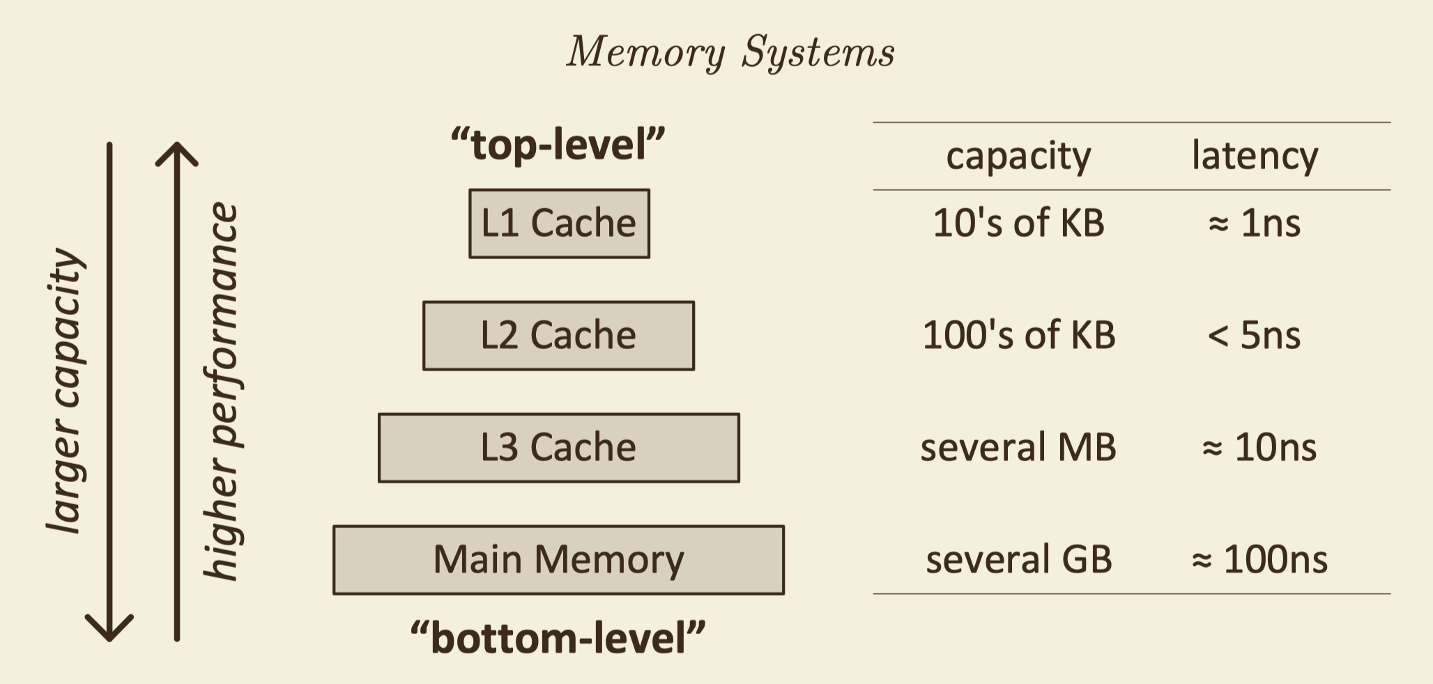
Memory Fundamentals
trade-off: price, capacity, performance
- if we fix price, then capacity and performance is zero-sum
- performance: latency, bandwidth, parallelism, \(bandwidth = parallelism/latency\)
multi-level memory system: because of the trade-off of memory, if we want both performance and capacity, we must use multi-level memory:
- cache: small but fast
- main memory: big bug slow
- disk: large and very slow
Cache
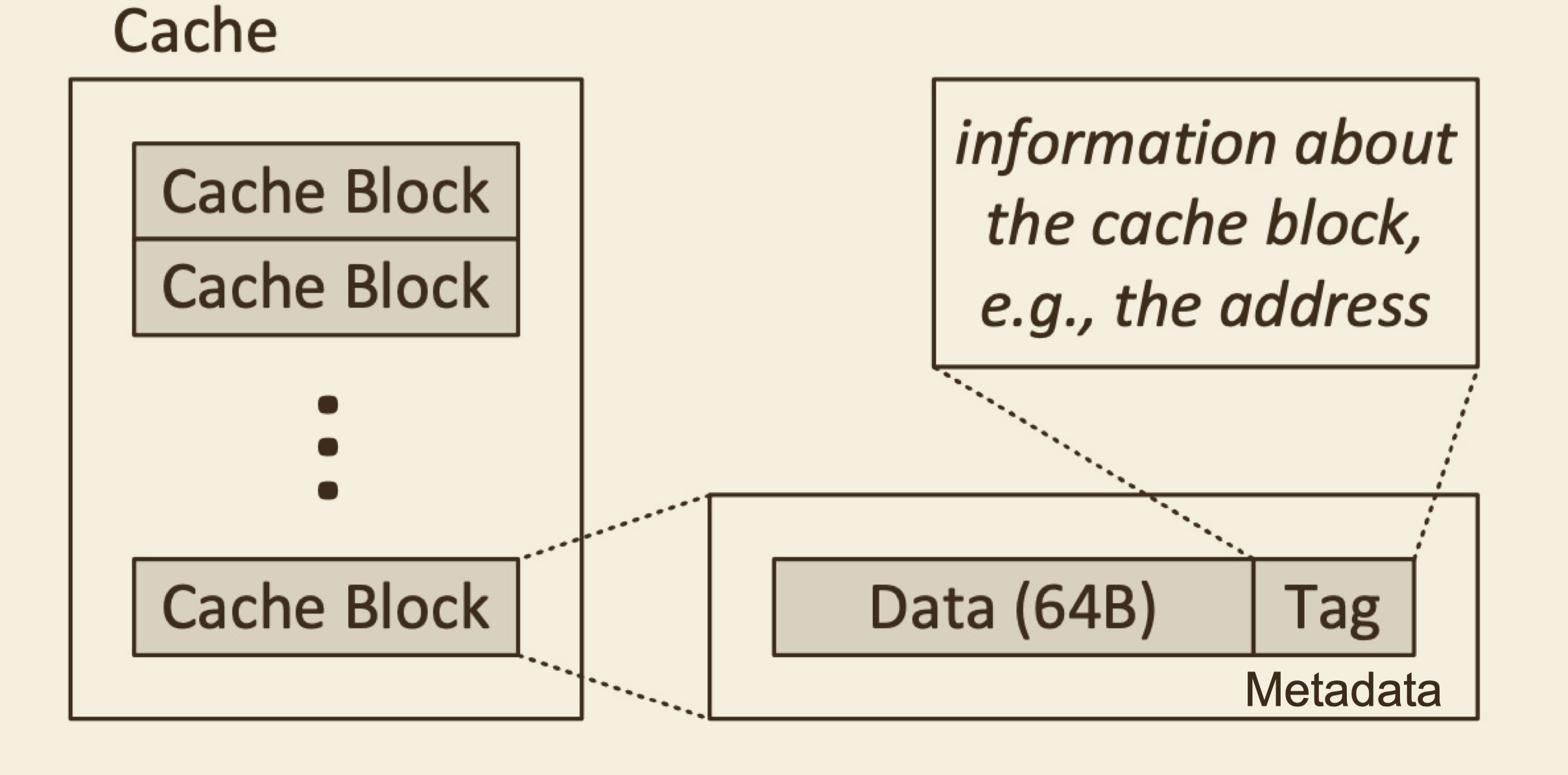
cache has a tag which is part of the main-memory address,
cache line may have other bits like: valid or dirtyL1 cache can be separated into I-Cache and D-Cache
- avoid instruction or data to occupy the whole cache and let the other has no cache
- pipeline constraints: I-cache and D-cache are used in
different parts of pipeline, when they are separate from each other,
both of them can be put near the hardware which need them most.
So both I-cache and D-cache access can be very fast. - latency if crucial for L1 cache, so L1 cache is small and has low
set-associative:
- L1 cache has to be fast to fit in the pipeline
- capacity grows, speed decrease
last level cache may be shared by multi-cores
- avoid only one core occupy the whole cache
- cache consistency
cache organization
- multi-level cache has the same data cache consistency check is very simple: only check the last level of cache is OK
- only one level of cache has the data, other level of cache don't has that data,
- mix of the above two method
manage policy:
- full-associative: main memory chunk can map into every cache block
- higher hit rate
- more complexity: more comparator, bigger mux
- bigger latency
- directly-mapped: memory chunk can only mapped into one specific cache block
- set-associative: memory chunk can only mapped into one set, but any
cache block inside that set. a W-way cache:
- W==N: full-associative
- W==1: directly-mapped
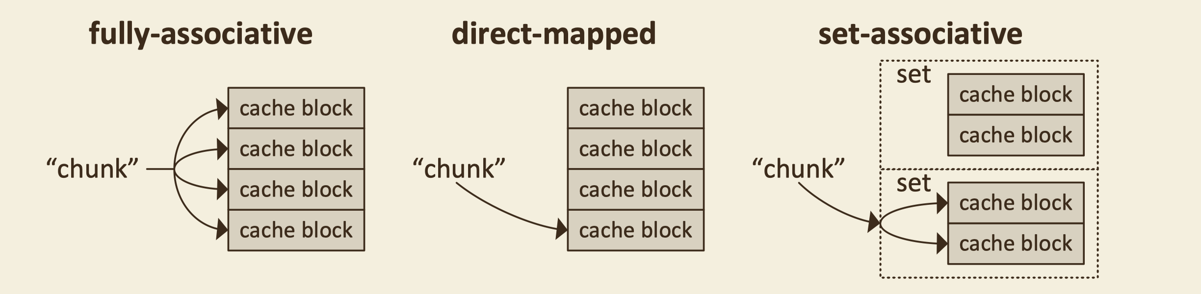
- full-associative: main memory chunk can map into every cache block
write handling:
- write through: when cache is write into, all higher level memory
must be write into
- easier for check cache consistency, prevents any data discrepancy from arising
- waste energy and bandwidth
- write back: write back to high level of memory only when evicting
- save energy and bandwidth
- more complicated when design cache
- need dirty flag
- write through: when cache is write into, all higher level memory
must be write into
use cache can reduce memory access time, the hit rate is very important in cache design,
but hit rate and capacity are zero-sum of access latency of cachetypes of cache miss:
- compulsory: the first time data is needed, prefetch can be helpful
- capacity: cash is too small <- better replacement policy
- conflict: X and Y have to use the same cache location <- higher associativity, better index algorithm
LRU:
- for N-way set-associative cache, you have to keep the order of N cache blocks in LRU algorithm
- method 1: each page-table entry has a counter, every time page is referenced through this entry, set the entry counter to clock -> the least recently used page has the smallest counter
- method 2: keep a stack of page numbers in double-link form -> page referenced,
- although LRU is probably not the best cache replacement policy, true
LRU is complexity to implement, so highly-associative processor don't
implement true LRU.
for example: in 2-way set-associative cache, suppose data sequence isABCABCABCthen random replacement policy is better than LRU replacement policy
improve cache performance
- improve hit rate
- more associativity
- better hashing
- better replacement policy
- software approaches
- reduce miss penalty
- multi-level cache
- crucial word first: when cache block is too large, don't wait the whole cache block, just feed the processor with most important words first to save time
- sub-blocking: divide the cache block to smaller sub-blocks, so the cache replacement can happen in sub-blocks
- software approaches
- improve hit rate
DRAM
1T1C: made of 1 transistor and 1 capacitor
- capacitor leaks, this is why DRAM is dynamic
- need refresh at least once in 64ms
- higher density than SRAM(6T)
- DRAM is in 2D structure, while NVEM is in 3D structure, DRAM can be 16 GB, while NVEM can be 2TB, but DRAM is 3000 times faster.
DRAM operations:
- Read
- row close
- pre-charge to 0.5 VDD
- row open
- sense-amplifier get the correct 0,1 of all bits in the row
- mux choose 8 bits of the row to output
- output driver write output the data get from the mux
ps: read operations is used as refresh of DRAM
- Write
- row close
- pre-charge to 0.5 VDD
- row open
- sense-amplifier get the correct 0,1 of all bits in the row
- mux choose 8 bits of the row to output
- input driver write the data into the mux, because input driver is stronger than sense-amplifier
- Read
sense-amplifier
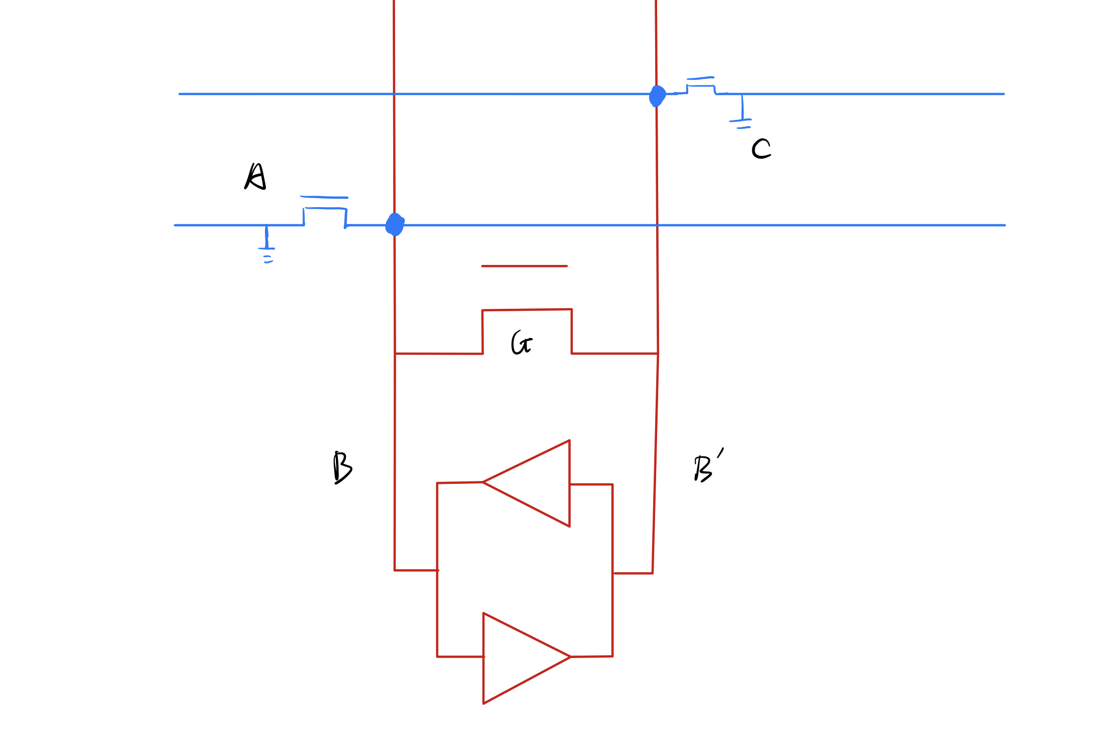
- differential pair: in DRAM, one row only attaches to one bit line of sense-amplifier, either B or B'
- in pre-charge, detach inverter of sense-amplifier, charge B to VDD, open G, then B and B' will both become VDD/2
- connect inverter of sense-amplifier, turn on one row,
sense-amplifier can read the stored data,
Example: suppose A is 1, then B will be charged to higher than VDD/2, which is eventually VDD,
and B' is eventually 0, because B is 1 and the bottom inverter will drive B' to 0 - besides, because B' is not connected to any store cell at this time, it will not influence other store cell
operations of DRAM is controlled by MC(memory controller)
- activate
- pre-charge
- read/write
level of DRAM
- channel: has unique address, control and data path
- rank
- bank
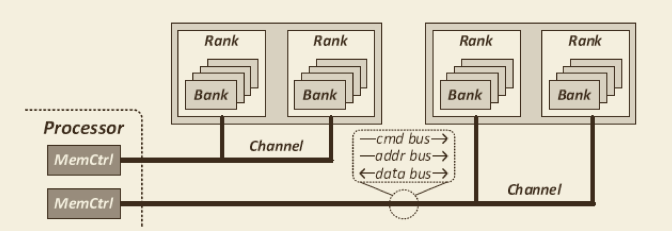
usually DRAM is not on chip, it's on motherboard
- high energy, long latency, low bandwidth
- 3D-Stacking: put DRAM on top of processor
PCM(phase charge memory) <- emerging memory technology
- Write data by pulsing current \(dQ/dt\)
- Read data by detecting resistance: high resistance for 1, low resistance for 0
- better scalable than DRAM, no need to refresh
- longer latency, short lifetime(can only write into a few times)
Virtual Memory
- programmer see virtual memory only:
- programmer don't know what hardware their program will running on, so they can't suspect the physical memory
- their are many programs running at the same time, programmer don't know the memory state when the program is running
- it's the OS to manage the mapping of virtual memory and physical
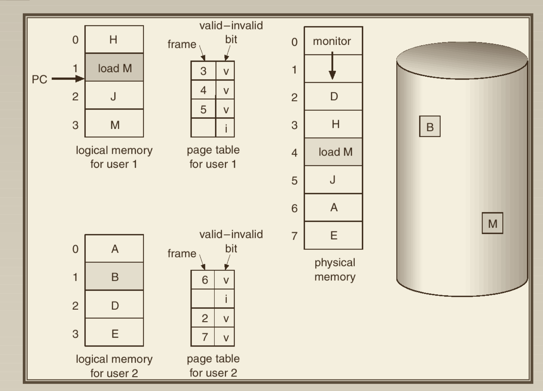
memory, the OS use Page Table to manage address mapping
- page table entry has valid bits to indicate if virtual memory is mapped to physical memory
- valid bit is 0 -> page fault -> trap to OS -> bring
in missing page -> update page table
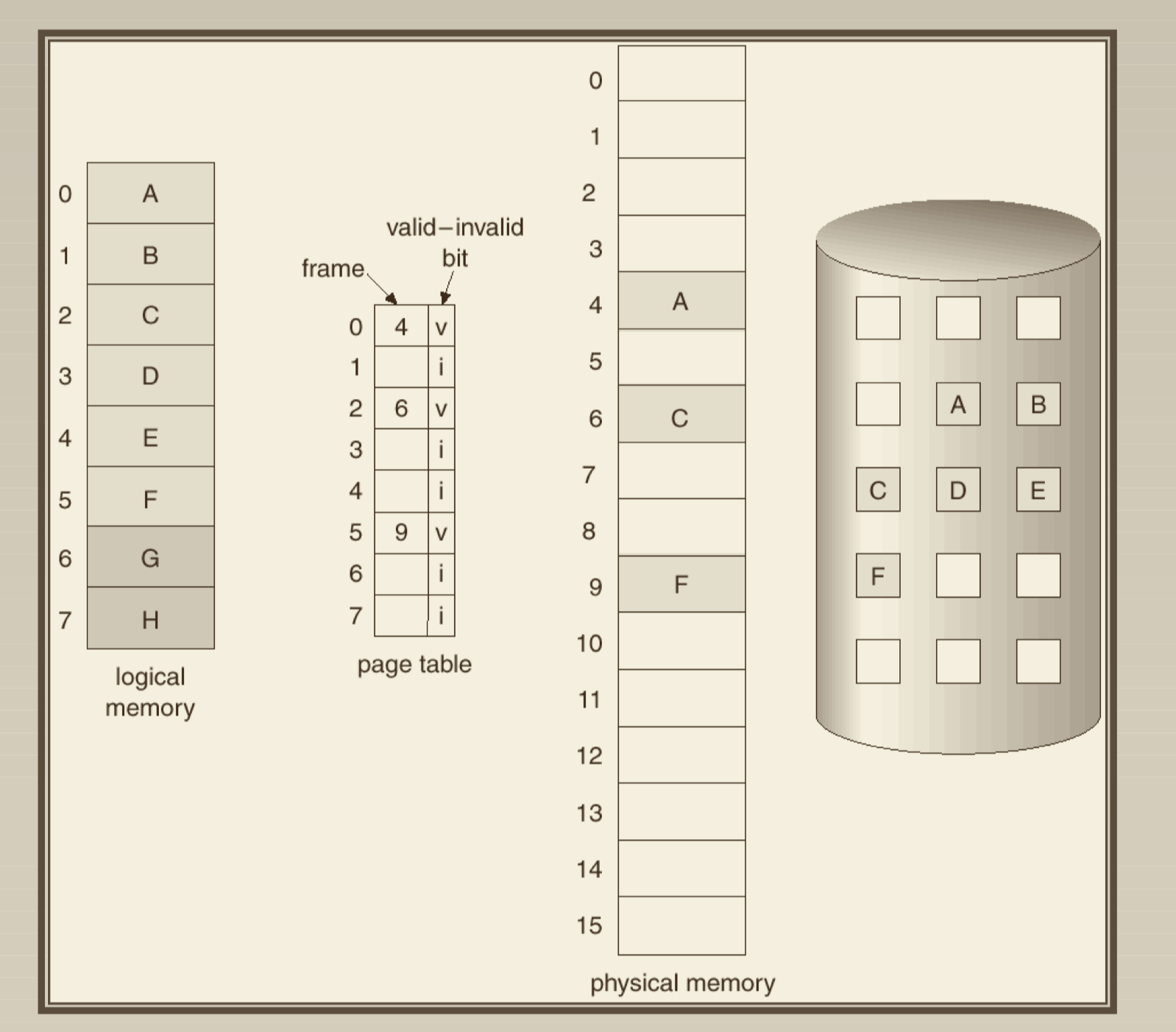
- page entry has dirty bits to indicate if the page in memory has been modified, when the page is evicted back to disk, only modified page will be write back
- page replacement algorithm: when physical frame is
full, we need an algorithm to choose a victim frame to swap out to disk.
- FIFO: will cause Belady's Anomaly(frame size grows, page fault grows)
- Optimal algorithm: can't implement this, we don't know the future move the page number to stack top
- for multi-user system, the OS has a page table for each user, so
each user can share the whole physical memory
- memory size can't be to small, or the complexity of manage virtual/physical mapping is difficult. modern processor has virtual memory page size equal to 4096 Byte
- we need TLB(which is a cache) to accelerate the translation from virtual memory to physical memory
- virtual memory space is much larger than physical memory space.
- trashing: if physical memory is too small, then some virtual memory page must be swap in and out, this will degrade system performance much
flash
nand flash: if you need big capacity(Gb, etc), nand is better
- less reliability, need high voltage to write into;
- cell will broken if you write to one cell to often. <- use ECC code to handle this problem
- ECC correction wastes time
nor flash: if you need small capacity(Mb, etc), nand is better
- less density than nand flash
- don't need to do ECC